HDI Printed Circuit Boards

HDI Printed Circuit Boards
What are HDI PCBs?
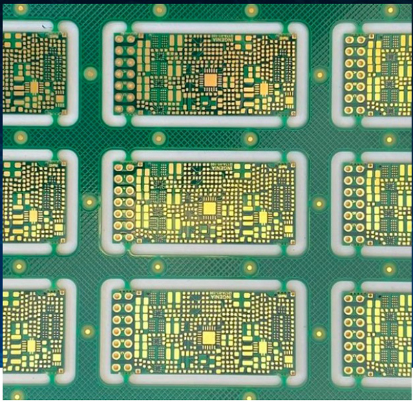
HDI Printed Circuit Boards (High Density Interconnect) are boards with a Higher Circuit density area than conventional PCB’s. HDI have finer lines and spaces, minor vias and capture pads and an increased connection pad density.
Due to the circuit density these board often require the use of fine traces to 0.075mm and complex designs may include blind and buried laser-drilled micro-vias to 0.1mm. Often using resin-filled plated over “in Pad Vias” to give a smooth planarized surface to solder to.
Components need to be placed on HDI boards with extreme precision due to the small size of the miniature pads. Special soldering techniques are required for the leadless chips which are often used with them and extra steps are required in the assembly process.
What are the advantages of HDI PCBs?
HDI boards are hugely versatile and are the perfect solution where space is at a premium.
They can withstand mechanical shocks extremely well due to their smaller size and lighter weight when contrasted with traditional rigid PCBs.
Using HDI Technology, designers have the ability to place more components in a smaller area allowing faster transmission of signals with a significant reduction in signal loss
HDI Boards are regularly used in Mobile Phones, Touch Screen Devices and 4G Network Communications and anywhere that space is at a premium.
Features of HDI PCBs
High Electrical Performance
High speed signal transmission rates are vital for many medical devices including implants, CT scanners and other monitoring equipment.
Fast
HDI technology delivers the high speed and frequency which is required in products such as personal computers, games consoles and mobile phones.
Lightweight
HDI printed circuit boards are smaller and lighter than standard boards. This makes them ideal for aerospace applications where weight savings are vital.
Reduced Size
HDI boards feature much greater circuit density which is achieved by blind vias, buried vias and microvias which are smaller than 0.15mm in diameter.
HDI PCB technical specification
|
Layers
|
4-22 layers
|
|
HDI builds
|
1+N+1, 2+N+2, 3+N+3,4+N+4, 5+N+5, 6+N+6, any layer in R&D
|
|
Features
|
Allows microvias to only penetrate select layers and also be placed on surface pads.
|
|
Materials
|
FR4 standard, FR4 high performance, Halogen free FR4, Rogers
|
|
Copper weights (finished)
|
18μm - 70μm
|
|
Minimum track and gap
|
0.075mm / 0.075mm
|
|
Minimum thickness
|
0.40mm
|
|
Maximum thickness
|
3.0mm
|
|
Surface finishes available
|
OSP, ENIG, Immersion tin, Immersion silver, Electrolytic gold, Gold fingers
|
|
Minimum mechanical drill
|
0.15mm
|
|
Minimum laser drill
|
0.10mm standard, 0.075mm advanced
|
|
Maximum dimensions
|
610mm x 450mm, depending upon laser drilling machine
|